 | –≠–ª–µ–∫—Ç—Ä–æ–Ω–Ω—ã–π –∫–æ–º–ø–æ–Ω–µ–Ω—Ç: UPC4742 | –°–∫–∞—á–∞—Ç—å:  PDF PDF  ZIP ZIP |
©
1998
DATA SHEET
BIPOLAR ANALOG INTEGRATED CIRCUIT
µ
PC4742
SINGLE SUPPLY VOLTAGE, HIGH SPEED,
WIDE BAND, DUAL OPERATIONAL AMPLIFIERS
The
µ
PC4742 is dual high speed, wide band operational amplifier designed for single supply operation from
+3 V to +32 V with low supply current drain. By using high speed PNP transistors for input and output circuits,
the excellent AC performance is achieved without degrading capacitive load drive capability.
With no crossover distortion and wide output voltage range characteristics, the
µ
PC4742 is optimum choice for
single supply AC amplifier, and active filters.
FEATURES
∑
High slew rate: 7 V/
µ
s TYP. (V
+
= +5 V, V
≠
= GND)
∑
Wide gain band width product: 3.5 MHz TYP. (V
+
= +5 V, V
≠
= GND)
∑
Wide supply voltage range: +3 V to +32 V
∑
Wide output voltage swing
∑
Common mode input voltage range includes V
≠
∑
Internal frequency compensation
∑
Output short circuit protection
Document No. G13958EJ1V0DS00 (1st edition)
Date Published December 1998 N CP(K)
Printed in Japan
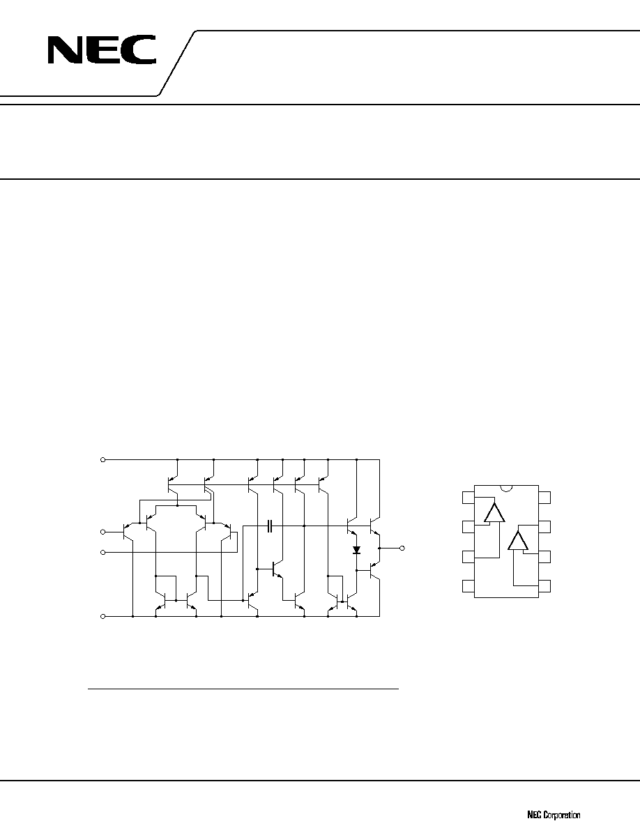
EQUIVALENT CIRCUIT (1/2 Circuit)
PIN CONFIGURATION
(Top View)
ORDERING INFORMATION
Part Number
Package
µ
PC4742C
8-pin plastic DIP (300 mil)
µ
PC4742G2
8-pin plastic SOP (225 mil)
The information in this document is subject to change without notice.
Q
7
Q
8
Q
9
Q
10
Q
11
Q
12
Q
18
Q
19
Q
20
Q
17
Q
16
Q
15
Q
13
Q
14
Q
6
Q
5
Q
2
Q
3
Q
4
Q
1
OUT
V
≠
I
N
I
I
V
+
1
2
3
4
8
7
6
5
V
+
OUT
2
I
I2
I
N2
OUT
1
I
I1
I
N1
V
≠
≠
+
≠
+
2
1
µ
PC4742C, 4742G2
µ
PC4742
2
ABSOLUTE MAXIMUM RATINGS (T
A
= 25
∞
C)
Parameter
Symbol
Ratings
Unit
Voltage between V
+
and V
≠
Note 1
V
+
≠V
≠
≠0.3 to +36
V
Differential Input Voltage
V
ID
±
36
V
Input Voltage
Note 2
V
I
V
≠
≠0.3 to V
≠
+36
V
Output Voltage
Note 3
V
O
V
≠
≠0.3 to V
+
+0.3
V
Power Dissipation
C Package
Note 4
P
T
350
mW
G2 Package
Note 5
440
mW
Output Short Circuit Duration
Note 6
Indefinite
sec
Operating Ambient Temperature
T
A
≠20 to +80
∞
C
Storage Temperature
T
stg
≠55 to + 125
∞
C
Notes 1. Reverse connection of supply voltage can cause destruction.
2. The input voltage should be allowed to input without damage or destruction independent of the
magnitude of V
+
. Either input signal should not be allowed to go negative by more than 0.3 V. The normal
operation will establish when the both inputs are within the Common Mode Input Voltage Range of
electrical characteristics.
3. This specification is the voltage which should be allowed to supply to the output terminal from external
without damage or destructive. Even during the transition period of supply voltage, power on/off etc.,
this specification should be kept. The output voltage of normal operation will be the Output Voltage Swing
of electrical characteristics.
4. Thermal derating factor is ≠5.0 mW/
∞
C when operating ambient temperature is higher than 55
∞
C.
5. Thermal derating factor is ≠4.4 mW/
∞
C when operating ambient temperature is higher than 25
∞
C.
6. Pay careful attention to the total power dissipation not to exceed the absolute maximum ratings, Note
4 and Note 5.
RECOMMENDED OPERATING CONDITIONS
Parameter
Symbol
MIN.
TYP.
MAX.
Unit
Supply Voltage (Split)
V
±
±
1.5
±
16
V
Supply Voltage (V
≠
= GND)
V
+
+3
+32
V
Output Current
I
O
±
10
mA
Capacitive Load (A
V
= +1, R
f
= 0
)
C
L
1000
pF
µ
PC4742
3
ELECTRICAL CHARACTERISTICS (T
A
= 25
∞
C, V
±
=
±
15 V)
Parameter
Symbol
Conditions
MIN.
TYP.
MAX.
Unit
Input Offset Voltage
V
IO
±
1.0
±
4.5
mV
Input Offset Current
I
IO
±
6
±
75
nA
Input Bias Current
Note 7
I
B
140
500
nA
Large Signal Voltage Gain
A
V
R
L
2 k
, V
O
=
±
10 V
25000
300000
Supply Current
I
CC
I
O
= 0 A, Both Amplifiers
4.3
5.5
mA
Common Mode Rejection Ratio
CMR
70
86
dB
Supply Voltage Rejection Ratio
SVR
70
93
dB
Output Voltage Swing
V
om
R
L
10 k
±
13.7
+14
V
≠14.3
Output Voltage Swing
V
om
R
L
2 k
±
13.5
V
Common Mode lnput Voltage Range
V
ICM
V
≠
V
+
≠1.8
V
Slew Rate (Rise)
SR
A
V
= 1, R
L
2 k
8.5
V
/µ
s
Gain Band Width Product
GBW
f
O
= 100 kHz
3.5
MHz
Channel Separation
f = 20 Hz to 20 kHz
120
dB
ELECTRICAL CHARACTERISTICS (T
A
= 25
∞
C, V
+
= 5 V, V
≠
= GND)
Parameter
Symbol
Conditions
MIN.
TYP.
MAX.
Unit
Input Offset Voltage
V
IO
±
1.0
±
5
mV
Input Offset Current
I
IO
±
6
±
75
nA
Input Bias Current
Note 7
I
B
160
500
nA
Large Signal Voltage Gain
A
V
R
L
2 k
25000
300000
Supply Current
I
CC
I
O
= 0 A, All Amplifiers
3.3
4.5
mA
Common Mode Rejection Ratio
CMR
70
80
dB
Supply Voltage Rejection Ratio
SVR
70
95
dB
Output Voltage Swing
V
om
R
L
2 k
(Connect to GND)
3.7
4.0
V
0
0
Common Mode lnput Voltage Range
V
ICM
0
V
+
≠1.8
V
Output Current (SOURCE)
I
O SOURCE
V
+
IN
= +1 V, V
≠
IN
= 0 V
10
30
mA
Output Current (SINK)
I
O SINK
V
+
IN
= 0 V, V
≠
IN
= +1 V
10
30
mA
Slew Rate (Rise)
SR
7
V
/µ
s
Notes 7. Input bias currents flow out from IC. Because each currents are base current of PNP-transistor on input
stage.
µ
PC4742
4
TYPICAL CHARACTERISTICS (T
A
= 25
∞
C, TYP.)
500
400
300
200
100
0
20
40
60
80
100
POWER DISSIPATION
T
A
- Operating Ambient Temperature - ∞C
P
T
- Total Power Dissipation - mW
V
IO
- Input Offset Voltage - mV
SUPPLY CURRENT
10
8
6
4
2
0
±5
±10
±15
±20
A
≠
+
V
≠
V
+
I
CC
T
A
= ≠20 ∞C
T
A
= +25 ∞C
T
A
= +80 ∞C
I
CC
- Supply Current - mA
200
150
100
50
0
10
20
30
40
INPUT BIAS CURRENT
40
30
20
10
0
10
20
30
40
V
+
- Supply Voltage - V (V
≠
= GND)
V
+
- Supply Voltage - V (V
≠
= GND)
COMMON MODE INPUT VOLTAGE RANGE
V
ICM
- Common Mode Input Voltage Range - V
V
ICM
+
V
ICM
≠
V
±
- Supply Voltage - V
5
4
3
2
1
0
≠1
≠2
≠3
≠4
≠5
≠50
0
100
50
T
A
- Operating Ambient Temperature - ∞C
INPUT OFFSET VOLTAGE
200
100
0
50
0
≠50
100
INPUT BIAS CURRENT
I
B
- Input Bias Current - nA
I
B
- Input Bias Current - nA
T
A
- Operating Ambient Temperature - ∞C
V
±
= ±15V
V
±
= ±15V
µ
µ
PC4742G2
PC4742C
227 ∞C/W
200 ∞C/W
µ
PC4742
5
120
100
80
60
40
20
0
10
100
1 k
10 k 100 k
1 M
10 M
A
V
- Open Loop Voltage Gain - dB
V
±
= ±15 V
OPEN LOOP FREQUENCY RESPONSE
f - Frequency - Hz
LARGE SIGNAL FREQUENCY RESPONSE
30
20
10
0
V
om
- Output Voltage Swing - V
p-p
100
1 k
10 k
100 k
1 M
10 M
V
±
= ±15 V
R
L
= 2 k
f - Frequency - Hz
10
1
0.1
0.01
0.01
0.1
1.0
10
100
I
O SINK
V
O
R
L
V
+
V
+
/2
The dotted line shows a
characteristic of R
L
= 1 k
OUTPUT SINK CURRENT LIMIT
I
O SINK
- Output Sink Current - mA
V
+
= 15 V
V
+
= 15 V
V
+
V
+
/2
≠
+
+
≠
I
O SOURCE
V
O
5
4
3
2
1
0
0.01
0.1
1.0
10
100
V
O
- Output Voltage - V
V
O
- Output Voltage to V
+
- V
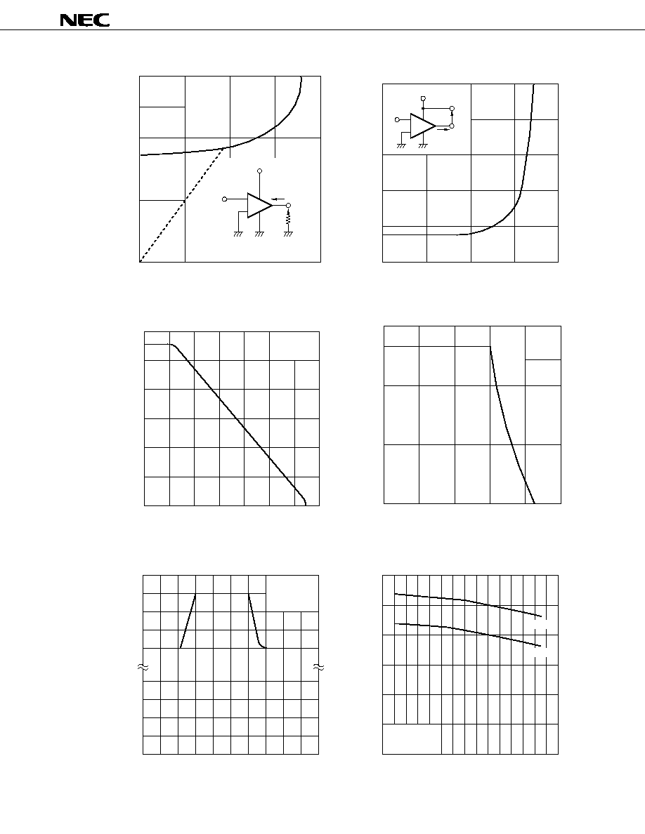
OUTPUT SOURCE CURRENT LIMIT
I
O SOURCE
- Output Source Current - mA
VOLTAGE FOLLOWER PULSE RESPONSE
3
2
1
0
3
2
1
0
0
1
2
3
t - Time - s
µ
µ
T
A
- Operating Ambient Temperature - ∞C
V
IN
- Input Voltage -V/V
O
- Output Voltage - V
R
L
= 2 k
V
+
= +5 V
V
≠
= GND
SLEW RATE
12
10
8
6
4
2
0
100
50
0
≠50
SR - Slew Rate - V/ s
SR
≠
SR
+
V
±
= ±15 V
R
L
= 2 k